


Advertisements


High Speed PCB
| Price: | US$ 10 |
|---|---|
| Minimum Order: | |
| Payment Terms: | T/T,Western Union, |
| Port of Export: |
Product Details
| Model No.: | Brand Name: |
|---|
| Certification: | |
|---|---|
| Specification: | / |
Packaging & Delivery
| Packaging: | |
|---|---|
| Delivery/Lead Time: | |
| Production Capacity: |
Product Description
Advantages of high-speed PCB:
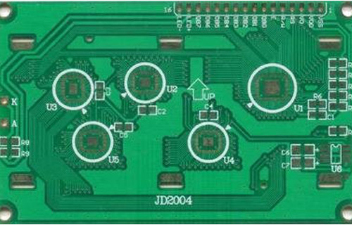
Multilayer PCB is generally used in high speed board design. Multilayer circuit boards are actually formed by laminating and bonding several etched single or double-sided boards. Compared with single-layer and double-layer circuit boards, multilayer circuit boards have many advantages, especially in small electronic products.
The assembly density of high-speed PCB boards is high and the volume is small. As the volume of electronic products becomes smaller and smaller, the electric property of high-speed PCBs also is under higher requirements, and the demand for multilayer circuit boards is also increasing.
The use of multilayer circuit boards facilitates wiring so that the wiring length is greatly shortened. And the wiring between electronic components is shortened, which also increases the speed of signal transmission.
For the high-frequency circuit, after the ground layer has been added, the signal line will form a constant low impedance to the ground so that the circuit impedance is greatly reduced, and the shielding effect is better.
For electronic products with high heat dissipation requirements, a high-speed PCB can be equipped with a metal-cored heat dissipation layer, which is convenient to meet the needs of special functions such as shielding and heat dissipation.
In terms of performance, the higher the number of layers is, the greater the production costs, and the relatively longer the processing time is, and the more complicated quality inspection is. However, under the cost comparison of the same area, although the cost of multilayer circuit boards is higher than that of single-layer and double-layer, the cost difference between the two is not so obvious when the noise reduction factor is concluded into consideration. As technology advances, PCB boards with more than 100 layers have already been used in sophisticated aerospace instruments and medical equipment.
The most common high-speed PCBs are the four-layer and the six-layer PCBs, which are used in computers that we are familiar with in daily life. The difference between the two kinds of PCBs above is that the six-layer PCB is thicker than the four-layer PCB because there are two signal layers are added between the ground layer and the power layer in the six-layer PCB. It’s easy to identify the single-layer and the double-layer PCBs with naked eyes. When holding the board under the light and looking at it, you will find the board is transparent except the traces on both sides. However, if there are no relative marks on the boards, it's not so easy to differentiate the four-layer and the six-layer PCBs.
When it comes to the overall high speed pcb layout, multilayer PCBs, with its flexible design, advantaged economy, stable electric property, and other advantages, have been widely applied to producing electrical productions.
SPEEDA Technology is a professional pcb board supplier. We provide Double Sided PCB, Multilayer PCB and so on. Want to know more? Please contact us.
图片链接:
https://*/uploads/image/20200527/high-speed-pcb.jpg
7、IMMERSION GOLD PCB / GOLD PLATING PCB / GOLD PLATED PCB
https://*/immersion-gold-pcb/
Immersion nickel/gold is a thick layer of nickel-gold alloy with good electrical properties and can protect the PCB for a long time. Unlike the OSP PCB Board, which is only used as a rust-proof barrier layer, it can be useful and achieve good electrical properties during long-term use of the PCB. In addition, immersion gold pcb also has environmental tolerance not available in other surface treatment processes.
Features of Immersion Gold PCB
The immersion gold board is a pcb board produced by the immersion gold process.
Such immersion gold boards are mostly multilayer PCB boards. The immersion gold process is to deposit a stable color on the surface of the printed circuit, good brightness, flat plating, and good solderability Nickel-gold plating, PCB can be used for a long time without oxidation problems.
It is mainly used on boards that have functional requirements for connection and long storage periods, such as the keypad area of a mobile phone, the edge connection area of a router housing, and the electrical contact area of a chip processor's elastic connection. Currently about 10% -20% of PCBs use the immersion nickel / gold process.
The general process is: de-acid cleaning-> micro-etching-> pre-immersion-> activation-> chemical nickel plating-> chemical immersion gold; there are 6 chemical tanks in the process, involving nearly a hundred Chemicals, the process is more complicated.
It is mainly used on boards that have functional requirements for connection and long storage periods, such as the keypad area of a mobile phone, the edge connection area of a router housing, and the electrical contact area of a chip processor's elastic connection. Currently about 10% -20% of PCBs use the immersion nickel / gold process.
PCB board has a variety of surface treatment methods, SPEEDAPCB is good at producing pcb boards with various surface treatment methods.
Parameters of Immersion Gold PCB
PCB SIZE 42 X 36mm=1PCS
BOARD TYPE Double sided PCB
Number of Layers 4 layers
Surface Mount Components YES
Through Hole Components YES
LAYER STACKUP Copper ------- 35um(1 oz)+plate TOP layer
RO4350B 0.254mm
Minimum Trace and Space: 7.1 mil / 5 mil
Minimum / Maximum Holes: 0.4 mm / 5.2 mm
Number of Different Holes: 6
Number of Drill Holes: 41
Number of Milled Slots: 0
Number of Internal Cutouts: 3
Impedance Control: No
Glass Epoxy of board: RO4350B Tg280ºC, er<3.48, Rogers Corp.
Final foil external: 1.5 oz
Final foil internal: N/A
Final height of PCB: 0.3 mm ¯0.1mm
Surface Finish Immersion gold
Solder Mask Apply To: TOP, 12micron Minimum
Solder Mask Color: Green, PSR-2000GT600D, Taiyo Supplied.
Solder Mask Type: LPSM
CONTOUR/CUTTING Routing
Side of Component Legend TOP
Colour of Component Legend White, IJR-4000 MW300, Taiyo brand
Manufacturer Name or Logo: Marked on the board in a conductor and leged
FREE AREA
VIA Plated through hole(PTH), minimum size 0.4mm.
FLAMIBILITY RATING UL 94-V0 Approval MIN.
Outline dimension: 0.0059"
Board plating: 0.0029"
Drill tolerance: 0.002"
TEST 100% Electrical Test
TYPE OF ARTWORK TO BE SUPPLIED Email file, Gerber RS-274-X, PCBDOC etc
SERVICE AREA Worldwide, Globally.
SPEEDA Technology is a professional printed circuit board company. We provide Double Sided PCB, Multilayer PCB and so on. Want to know more? Please contact us.
|
SUPPLIER PROFILE
|
|||
|---|---|---|---|
| Company: | Hunan Speeda Technology Co.,Ltd. | ||
| City/State | Changsha, | Country: |
China 
|
| Business Type: | Export - Manufacturer / Trading Company | Established: | NA |
| Member Since: | 2021 | Contact Person | Molly Tu |
SUPPLIER PROFILE
City/State/Country -
Changsha,
China
Business Type -
Export - Manufacturer / Trading Company
Established -
NA
Member Since -
2021
Contact Person -
Molly Tu