


")
Advertisements


HDI PCB / BLIND&BURIED VIA HOLE PCB / BVH PCB
| Price: | US$ 10 |
|---|---|
| Minimum Order: | |
| Payment Terms: | T/T,Western Union, |
| Port of Export: |
Product Details
| Model No.: | Brand Name: |
|---|
| Certification: | |
|---|---|
| Specification: | / |
Packaging & Delivery
| Packaging: | |
|---|---|
| Delivery/Lead Time: | |
| Production Capacity: |
Product Description
SPEEDAPCB has been focusing on the production of various PTH (plated through hole PCB), buried via hole PCB and blind via hole PCB, and hdi pcb prototype.
When it comes to blind and buried hole circuit boards, everyone thinks of HDI boards. Generally, there are more blind and buried hole circuit boards used in mobile phones or navigation instruments. Such PCB boards require high technical content and accurate accuracy. Of course, the price is compared with other It is also high for multilayer circuit boards.
HDI high density interconnect pcb : 1 + n + 1, 1 + 1 + n + 1 + 1, 2 + n + 2, 3 + n + 3,
Features of Blind&Buried Via Hole PCB
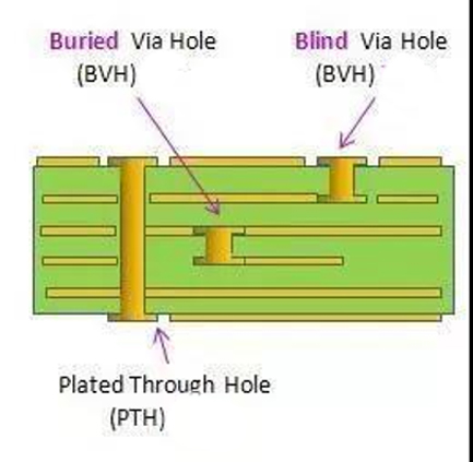
Blind Via Hole is the connection between the outermost circuit in the PCB and the adjacent inner layer with a plated hole. Because the opposite side cannot be seen, it is called blind pass. In order to increase the space utilization between the circuit layers of the board, blind holes come in handy. The blind hole is a via hole to the surface of the printed board.
Buried Via Hole, the connection between any circuit layers in the PCB, but there is no conduction with the outer layer, that is, there is no meaning of a via hole extending to the surface of the circuit board.
The blind holes are located on the top and bottom surfaces of the circuit board and have a certain depth. They are used to connect the surface layer circuits to the inner layer circuits below. The depth of the holes generally has a prescribed ratio (aperture). This manufacturing method requires special attention, and the drilling depth must be just right. Failure to pay attention will cause difficulties in plating inside the hole. Therefore, few factories will adopt this production method. In fact, it is possible to drill the holes of the circuit layers that need to be connected beforehand, and then glue them together, but they need more precise positioning and alignment devices.
This manufacturing process cannot be achieved by bonding the circuit boards and then drilling. It is necessary to perform the drilling operation at the individual circuit layer, firstly locally bond the inner layer, then perform plating treatment, and finally all the bonding. Because the operation process is more laborious than the original vias and blind holes, the price is also the most expensive. This manufacturing process is usually only used for high-density circuit boards, increasing the space utilization of other circuit layers.
In the PCB manufacturing process, drilling is very important. The simple understanding of drilling is to drill the required via holes on the copper clad board, which has the function of providing electrical connections and fixing devices. If the operation of the via is caused by incorrect operation, the device cannot be fixed on the circuit board, which will affect the use of the circuit board, and the entire board will be scrapped. Therefore, the process of drilling is very important.
Parameters of Blind&Buried Via Hole PCB
Items Capability.
Max board size 580X700mm
Boar Material FR-4,Aluminum, High Tg FR4,CEM3,etc.
Min trace width/ space (inner layer) 4mil/4mil(0.1mm/0.1mm)
Min PAD (inner layer) 5 mil(0.13mm)
Min thickness(inner layer) 4 mil(0.1mm)
Inner copper thickness 0.5~4 oz
Outer copper thickness 0.4~6 oz
Finished board thickness 0.4-3.2 mm
Board thickness tolerance control ¯0.10 mm ¯0.10 mm
¯10% ¯10%
¯10% ¯10%
Inner layer treatment brown oxidation
Layer count Capability 1-30 LAYER
alignment between ML ¯2mil
Drill hole diameter 0.15mm-0.65mm
Aspect ratio of plated hole 10:01
Hole precision ¯2 mil(¯0.05mm)
tolerance for Slot ¯3 mil(¯0.75mm)
Hole diameter tolerance(PTH) ¯3 mil(¯0.075mm)
Hole diameter tolerance(NPTH) ¯1mil(¯0.025mm)
Max Aspect Ratio for PTH 8:01
Hole wall copper thickness 15-50um
Alignment of outer layers 4mil/4mil
Min trace width/space for outer layer 4mil/4mil
Tolerance of Etching +/-10%
Thickness of solder mask on trace
Thickness of solder mask at trace corner ≥0.2mil(5um)
Hardness of solder mask On base material ≤+1.2mil
6H Finished thickness
Alignment of solder mask film ¯2mil(+/-50um)
Min width of solder mask bridge 4mil(100um)
Max hole with solder plug 0.5mm
Surface treatment HAL (Lead or Lead free), immersion Gold, Immersion Nickel, Electric Gold finger, plated Gold, OSP, Immersion Silver.carbon oil,etc.
Max Nickel thickness for Gold finger 280u"(7um)
Max gold thickness for Gold finger 30u"(0.75um)
Nickel thickness in Immersion Gold 120u"/240u"(3um/6um)
Gold thickness in Immersion Gold 2u"/6u"(0.05um/0.15um)
Impedance control and its tolerance 50¯10%,75¯10%,100¯10% 110¯10%
Trace Anti-stripped strength ≥61B/in(≥107g/mm)
bow and twist 0.75%
SPEEDA Technology is a professional printed circuit board supplier. We provide Double Sided PCB, Multilayer PCB, hdi pcb board, hdi printed circuit boards, hdi circuit boards, buried via pcb, buried vias pcb and so on. Want to know more? Please contact us.
|
SUPPLIER PROFILE
|
|||
|---|---|---|---|
| Company: | Hunan Speeda Technology Co.,Ltd. | ||
| City/State | Changsha, | Country: |
China 
|
| Business Type: | Export - Manufacturer / Trading Company | Established: | NA |
| Member Since: | 2021 | Contact Person | Molly Tu |
SUPPLIER PROFILE
City/State/Country -
Changsha,
China
Business Type -
Export - Manufacturer / Trading Company
Established -
NA
Member Since -
2021
Contact Person -
Molly Tu