


Advertisements


GaAs(Gallium Arsenide)Wafer
| Price: | Contact for latest price |
|---|---|
| Minimum Order: | |
| Payment Terms: | N/A |
| Port of Export: |
Product Details
| Model No.: | Brand Name: |
|---|
| Certification: | |
|---|---|
| Specification: | N/A |
Packaging & Delivery
| Packaging: | |
|---|---|
| Delivery/Lead Time: | |
| Production Capacity: |
Product Description
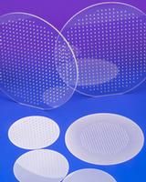
PAM Develops and manufactures compound semiconductor substrates-gallium arsenide crystal and wafer.We has used advanced crystal growth technology,vertical gradient freeze(VGF) and GaAs wafer processing technology,established a production line from crystal growth, cutting, grinding to polishing processing and built a 100-class clean room for wafer cleaning and packaging. Our GaAs wafer include 2~6 inch ingot/wafers for LED,LD and Microelectronics applications.
GaAs epi wafer,GaAs HEMT,GaAs mmic,GaAs pHEMT,InP HEMT
epi wafer
|
SUPPLIER PROFILE
|
|||
|---|---|---|---|
| Company: | Xiamen Powerway Advanced Material Co.,Limited | ||
| City/State | Xiamen, Fujian | Country: |
China 
|
| Business Type: | Export - Manufacturer / Trading Company | Established: | 1999 |
| Member Since: | 2013 | Contact Person | Victor Chan |
SUPPLIER PROFILE
City/State/Country -
Xiamen, Fujian
China
Business Type -
Export - Manufacturer / Trading Company
Established -
1999
Member Since -
2013
Contact Person -
Victor Chan