


Advertisements


Blind Via PCB
| Price: | US$ 1 / Bag |
|---|---|
| Minimum Order: | |
| Payment Terms: | TT |
| Port of Export: |
Product Details
| Model No.: | Brand Name: |
|---|
| Certification: | |
|---|---|
| Specification: | Blind Via PCB |
Packaging & Delivery
| Packaging: | |
|---|---|
| Delivery/Lead Time: | |
| Production Capacity: |
Product Description
ZF Electronics, as one of the top custom circuit board manufacturers and pcb manufacturing companies in China, can provide customers with single-sided PCB, double-sided FR4 PCB, metal core PCB, heavy copper PCB, rigid PCB and rigid-flex PCB.
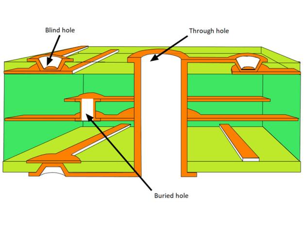
As the name suggests, blind via cannot be seen. Blind via buried viais the via that connects the surface layer and the inner layer without penetrating the entire board. In order to increase the space utilization of the PCB circuit layer, the blind via is produced. Blind via in pcb is located on the top and bottom surfaces of the printed circuit board and has a certain depth. It is used to connect the surface circuit and the underlying inner circuit and the depth of the hole usually does not exceed a certain ratio (aperture).
How to manufacture blind via PCB?
The hdi vias PCB production method requires special attention to the depth of the drilling (Z-axis) to be just right. If you do not pay attention to it, it will cause difficulties in electroplating in the via, so almost no factory adopts it. You can also put the circuit layer that needs to be connected in advance in the individual circuit layer. The blind and buried vias are drilled first, and then glued together, but more precise positioning and alignment devices are required.
The line width and line spacing of most process equipment: blind via 0.1mm, 0.125mm, 0.15mm.
Difference between blind via and plating through blind via hole PCB
From the processing point of view, through hole circuit board PCB and blind via and buried via hole PCB have different requirements for cutting tools in terms of chip removal ability. The processing of blind buried vias makes it easy for the cutting tool to be buried in iron chips, so better chip removal performance is required.
It is better to use spiral flute taps to machine blind holes, instead of straight flutes, it is easy to block chips and cause tool breakage.
For drilling and blind hole processing, it is best to use an internally cooled central water outlet drill bit. With the central water outlet effect of the machine tool, the iron filings can be forced off by the coolant pressure, so that the iron filings will not be entangled and blocked, which leads to over-tolerance in machining and breakage of tools.
The boring is the same as the drilling, and it is best to use the center outlet.
But the above statement is not absolute espeically when you want custom made pcb boards. It mainly depends on the depth-to-diameter ratio of the blind via aspect ratio. If the shallow hole is processed, it can also be used as a general plating through hole PCB processing tool.
If you have questions about our blind via PCB production capacity, or the specifications required for your custom project are not listed on this page, please feel free to contact us. We will reply within one workday. We will continue to provide quotation support and design support. Welcome to learn about our production process.
|
SUPPLIER PROFILE
|
|||
|---|---|---|---|
| Company: | Zhongfeng Electronics Co., Ltd. | ||
| City/State | shenzhen, | Country: |
China 
|
| Business Type: | Export - Manufacturer / Trading Company | Established: | NA |
| Member Since: | 2021 | Contact Person | zf pcba |
SUPPLIER PROFILE
City/State/Country -
shenzhen,
China
Business Type -
Export - Manufacturer / Trading Company
Established -
NA
Member Since -
2021
Contact Person -
zf pcba